The surface mount assembly PCB assembly process starts with the selection of the components and creating PCB layouts using various software packages. The components for the PCB assembly are packaged in different ways such as tubes, reels, and trays. After these preliminary steps, the SMT PCB assembly process proceeds through the following steps:
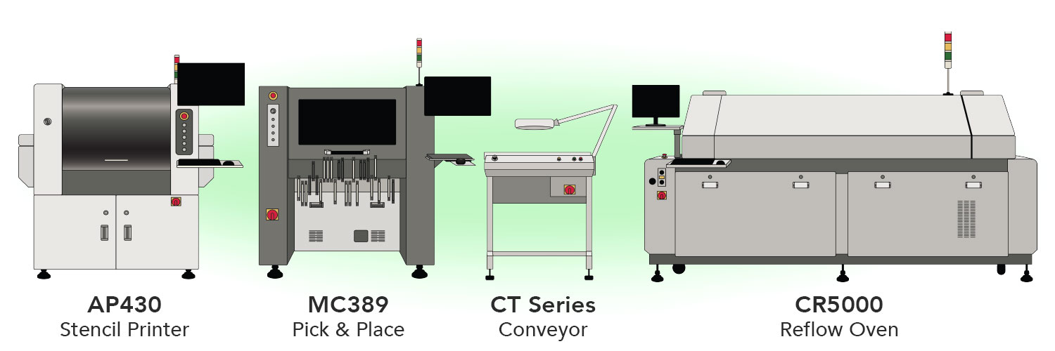
- Solder Paste Printing: The actual PCB assembly process begins here. Solder paste is applied to the PCB pad using a solder paste printer. The printer uses a stencil and squeezes the appropriate amount on the pad. This step forms the basis of PCB assembly, so, if anything goes wrong here, more defects will follow.
- Inspection of Solder Paste: The solder paste inspection is performed using a built-in solder paste inspection system or a separate inspection system. This inspection allows PCB designers to check solder paste volume on the pad and print area, and so on.
- Placement of Components: This step follows after PCB printing. All components are picked directly from their packaging using a gripper or vacuum nozzle, checked for appropriateness, and placed on the printed area at a high speed.
- Inspection: Although the pick and placement machines are automated, it is important to inspect component placement before proceeding to reflow soldering. AOI machines are used for inspection of placement. They help identify the component presence, positioning, polarities, and value.
- Reflow Soldering: This step follows the inspection of components. Electrical solder connections are made by heating the assembly to a pre-set temperature. Upon accomplishing all the above steps, reflow soldering may seem as a simple step. However, this is one of the most challenging steps because achieving the correct reflow profile is important. Any increase or decrease in temperature may damage solder joints.
- Reflow Soldering Inspection: AOI inspection is conducted to check the quality of soldered joints. Along with this, X-ray inspection is also performed to check BGA component packages, voids or broken solder joints, and so on.